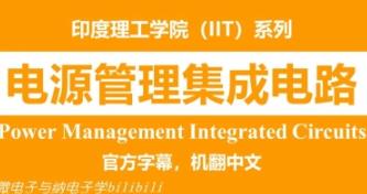
- 00 Introduction - Power Management Integrated Circuits
- 01 Introduction to PMIC - Part 1
- 02 Introduction to PMIC - Part 2
- 03 Linear versus Switching Regulators
- 04 Performance Parameters of Regulators
- 05 Local vs Remote Feedback Point of Load Regulators
- 06 Kelvin Sensing Droop Compensation
- 07 Current Regulator Applications Introduction to Bandgap Voltage References P
- 08 Adding PTAT and CTAT Voltages
- 09 Bandgap Voltage Reference Circuit Brokaw Bandgap Circuit
- 10 Sub-1-volt Bandgap Circuit
- 11 Generating Multiple Reference Voltages; Applications of Linear Regulators
- 12 Designing a Linear Regulator Negative and Positive Feedback
- 13 First Order Systems Phase Margin
- 14 Closed-Loop Response of Second Order Systems
- 15 Relationship between Damping Factor and Phase Margin Frequency Compensation
- 16 Finding the Poles of the Error Amplifier Part 1
- 17 Finding the Poles of the Error Amplifier Part 2
- 18 Dominant Pole Frequency Compensation
- 19 Dominant Pole Compensation at No-Load
- 20 Dominant Pole Compensation using Miller Effect RHP zero due to Miller Capaci
- 21 Intuitive Method of Finding the Poles Pole Splitting after Miller Compensati
- 22 Effect of RHP zero on Stability Mitigating the Effect of RHP zero LDO with
- 23 Output Impedance of PMOS LDO
- 24 Line Regulation and PSRR of PMOS LDO
- 25 PSRR of PMOS versus PSRR of NMOS LDO
- 26 Sources of Error in Linear and Switching Regulators
- 27 Offset in Amplifiers; Real Life Analogy; Static Offset Cancellation
- 28 Dynamic Offset Cancellation Techniques Chopping Auto zeroing
- 29 Digital LDO Technique to Avoid Limit Cycle Oscillations in Digital LDO
- 30 Hybrid LDO Short-Circuit Protection
- 31 Hiccup Mode and Foldback Current Limit
- 32 Introduction to Switching Regulators
- 33 volt-second Balance Non-Idealities in the Power Stage of a Buck Converter
- 34 Transformer Model of Buck Conduction Efficiency Efficiency of an LDO vs. Sw
- 35 Synchronous versus Non-Synchronous Switching Regulators PWM Control Techniqu
- 36 Losses in Switching Regulators (Conduction Loss Gate-Driver Switching Loss)
- 37 Dead-Time Switching Loss in DC-DC Converters
- 38 Hard Switching Loss in DC - DC Converters
- 39 Magnetic Loss in DC - DC Converters Relative Significance of Losses as a Fun
- 40 Output Voltage Ripple of a Buck Converter
- 41 Choosing the Inductor and Capacitor of a Buck Converter
- 42 CCM Vs DCM Operation in DC - DC Converters
- 43 CCM - DCM Boundary Condition Voltage Conversion Ratio in DCM
- 44 Concept of Pulse Frequency Modulation PFM
- 45 Classification of Pulse Width Modulators
- 46 DC - DC Converter Control Techniques Stability Analysis of Voltage Mode Buck
- 47 Stability Analysis of Voltage Mode Buck Converter Part 2
- 48 Stability Analysis of Voltage Mode Buck Converter Part 3
- 49 Dominant Pole Compensation (Type-I with Gm-C Architecture)
- 50 Dominant Pole Compensation (Type-I with Op Amp-RC Architecture)
- 51 Introduction to Type-II Compensation
- 52 Type-II Compensator using Gm-C Architecture - Part 1
- 53 Type-II Compensator using Gm-C Architecture - Part 2
- 54 Type-II Compensator using Gm-C Architecture - Part 3
- 55 Type-II Compensator using Op Amp-RC Architecture
- 56 Introduction to Type-III Compensator
- 57 Type-III Compensator using Op Amp-RC Architecture
- 58 Simulation of DC-DC Converter with Type-III Compensator
- 59 Type-III Compensator using Gm-C Architecture
- 60 Feed-Forward Line Compensation Loop Gain Compensation by Modulating Gm
- 61 Designing a Buck Converter Power Loss Budgeting
- 62 Sizing Power MOSFETs
- 63 Estimating Switching Losses and Choosing the Switching Frequency
- 64 Choosing Inductance and Capacitance Values
- 65 Choosing C Depending on Factors that Limit the Load Transient Response
- 66 Inductor and Capacitor Characteristics Reducing the Effect of Capacitor ESL
- 67 Gate Buffer and Non-Overlap Clock Generator in Gate-Driver Circuit
- 68 Pulse-Width Modulator- Trailing Edge Leading Edge and Dual Edge; Triangle Wa
- 69 Average Ramp Voltage of Single-Edge PW ModulatorDesign Considerations of EA
- 70 Delays Associated with PW Modulator PFM and PSM Operation DCM Operation usi
- 71 Designing a Zero-Cross Comparator Inverter-Based Auto-Zeroed Comparator Sim
- 72 Current Mode Control- Peak Valley Emulated; VMC versus CMC; Sub-Harmonic Os
- 73 Ramp-Adaptive Slope Compensation to Avoid Current Loop Instability
- 74 Non-Linear Control of DC-DC Converters Phase-Shift between i_L and v_C
- 75 Stabilising a Voltage-Mode Hysteretic Converter using R_esr
- 76 Hysteretic Converter - Simulation Demo
- 77 Current-Mode Hysteretic Converter Using R-C as Ripple Generator
- 78 Controlling the Switching Frequency of a Hysteretic Converter Delay in the H
- 79 Frequency and Voltage Regulation Loops in a Fixed-Frequency Hysteretic Conver
- 80 Resetting the Capacitor Voltage in a Hysteretic Converter Constant ON-Time C
- 81 Introduction to Boost Converter RHP Zero in a Boost Converter
- 82 Introduction to Buck-Boost Converter
- 83 Tri-Mode Buck-Boost Converter (Buck Buck-Boost and Boost)
- 84 Boundary Conditions for Mode Transition in a Tri-Mode Buck-Boost Converter
- 85 Generating Buck and Boost Duty Cycles in a Tri-Mode Buck-Boost Converter
- 86 Introduction to Switched-Capacitor DC-DC ConvertersSwitched-Capacitor DC-DC
- 87 Applications of Switched-Capacitor DC-DC Converters in Open-Loop
- 88 H-Bridge Switched-Capacitor DC-DC ConverterSC DC-DC converter with Multiple
- 89 Current Sensing Techniques in DC-DC Converters
- 90 Analog Layout Techniques - Part 1
- 91 Analog Layout Techniques - Part 2
- 92 Digital Control of DC-DC Converters ADC Architectures
- 93 Digital Pulse-Width Modulator Architectures Adaptive Compensation
- 94 Limitations of Analog and Digital Controllers Time-Based Controller for Buck
- 95 Time-Based Controller for Buck Converter and for LDO Issues with Time-Based
- 96 Multi-Phase DC-DC Converters
- 97 Dynamic Voltage and Frequency Scaling Single Inductor Multiple Output (SIMO)
- 98 LCDAMOLED Display Drivers - Part 1
- 99 LCDAMOLED Display Drivers - Part 2
- 100 LCDAMOLED Display Drivers - Part 3
- 101 LED Drivers for Camera Flash
- 102 Li-Ion Battery and its Charging Phases
- 103 Battery Charger IC
印度理工学院 - 电源管理集成电路:从理论到实践的工程必修课
【课程描述】
这门由印度理工学院开发的《电源管理集成电路》课程,是电力电子领域不可多得的实战型教学内容。不同于传统理论课,课程直接从工程应用角度切入,涵盖DC-DC转换器、LDO稳压器、电池管理系统等核心模块的设计要点。我特别欣赏课程中"手撕Datasheet"的环节——通过逆向分析TI/ADI等大厂的芯片手册,教会学生快速掌握商业级PMIC设计的关键参数。

实验部分尤其硬核,使用Cadence Virtuoso完成全流程设计仿真。记得有个学员分享过,他在完成Buck变换器布局时,突然意识到课本上的效率计算公式需要叠加PCB寄生参数才算准确——这正是课程强调的"真实世界工程思维"。
近年新增的汽车电子电源案例非常实用,比如如何处理发动机启停时的电压突变问题。课程采用的"问题-方案-优化"三段式教学法,特别适合想要突破"会仿真但调不通电路"瓶颈的工程师。最后一章的芯片测试环节,甚至会演示如何用示波器捕捉纳秒级开关噪声。
学习目标
掌握四大核心能力
- PMIC架构选型:根据应用场景选择最优拓扑结构
- 关键参数计算:纹波、效率、热损耗的工程级估算
- EDA工具实战:Cadence+LTspice协同设计流程
- 故障诊断:使用有限设备快速定位电源故障

课程大纲
模块一:基础构建(42课时)
- 开关电源工作原理深度剖析
- MOSFET驱动电路的12个设计陷阱
- 磁性元件选型指南(含铁氧体/合金粉末对比)
模块二:进阶设计(36课时)
- 多相位VRM设计要点
- 汽车电子EMC整改案例
- 低静态电流设计技巧
模块三:工程实战(24课时)
- 基于STM32的数控电源开发
- 芯片级热仿真与散热方案
- 量产测试方案设计
这门课最适合谁学?
如果你正在从事以下工作,会获得立竿见影的提升:硬件工程师(1-3年经验)、电动汽车BMS开发人员、消费电子电源设计师。课程对模电基础有一定要求,建议先掌握运放、反馈系统等基础知识。
来自深圳某无人机公司的学员反馈,学完LDO章节后,他们团队把产品待机电流从500μA优化到了80μA——这正是课程强调的"每微安都值得争取"的电源设计哲学。